Celebrating the 76th anniversary of the founding of the People’s Republic of China and the Mid Autumn Festival!
Wishing all Chinese around the world a happy holiday!
Wishing all Chinese around the world a happy holiday!
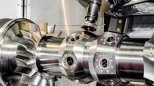
01 Advantages of Ceramic BladesHard alloy cutting tools encounter...
Dry machining is one of the important development trends...
~Abandoning the complexity of multiple cutting tools, only one...
Wishing all Chinese around the world a happy holiday!
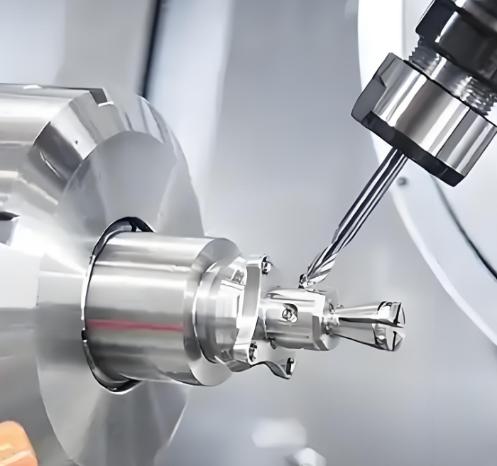
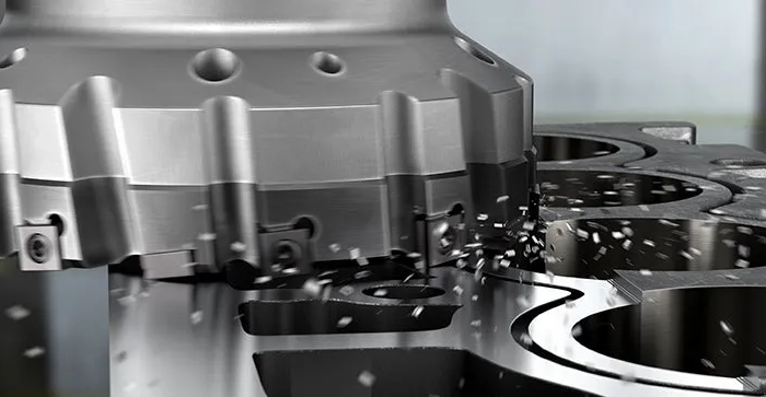
01 Advantages of Ceramic BladesHard alloy cutting tools encounter...
Dry machining is one of the important development trends...
~Abandoning the complexity of multiple cutting tools, only one...